


Thanks for visiting our updated website!
I am optimistic. Corporate Sustainability Initiatives have recently made their way to the Boardrooms of many Semiconductor manufacturers. Aggressive goals for Water, Chemical, and Rare Earth reductions have been outlined. I am hopeful this movement can result in real change; that IC manufacturers are inspired to address the root causes of waste within unit processes like CMP. Historically, copy exactly semiconductor manufacturing culture has not been able to move the consumption needle significantly. 300mm wafers require the same 7.75 KG of water per square cm as 200mm wafers did. Manufacturers spend proportionally more ($1.8 Billion annually) on CMP slurry while less than 10% of it ever touches a wafer... In 2020 Global Semiconductor manufacturing used well over 100 Billion gallons of water, "each fab using as much as a small city". I am optimistic that the industry is truly taking Sustainability seriously and that fabs can drive greater ecological efficiency.
I would love to demonstrate how to reduce your usage and CMP footprint over 30% through our economical approach.
Steve Benner
President, Confluense
Welcome to Confluense.
Confluense LLC is a CMP Technology Company which was born out of a simple observation. Most all of the fresh slurry added throughout the process rolls around the wafer carrier in a 'bow wave'. The material utilization and polishing efficiency of the process is governed by the equipment's global mixing technique.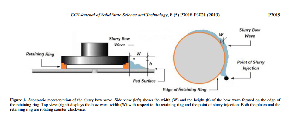 Once a CMP polishing pad is charged with slurry there is no competent mechanism to exhaust or exchange the spent slurry material contained within its surface texture. Practitioners feed fresh slurry overtop of a saturated pad and rely on mixing at the wafer carrier interface to maintain slurry 'slip stream' uniformity. This method's utilization efficiency (amount of fresh raw material that participates in the process) is less than 10%. In other words, less than 10% of the slurry flowing into the polisher ever sees the workpiece. Yikes!
We identified a simple fix: Physically remove the spent slurry from the upper surface of the pad as it exits the wafer and enable this displaced volume to be replenished with fresh slurry. This exhaust and exchange of the polishing film results in much more uniform process conditions within the "polishing chamber" (interfacial region between the wafer and pad). Our Controlled Fluid Residence technique both: intensifies the process - providing 10% -15% greater throughput, and exhausts many common sources of defects - resulting in 70% reductions in scratch and chatter marks.

Finally, perhaps counter intuitively, the active removal of spent materials from the pad surface actually requires less slurry supply, because the vacated region is recharged at 100% efficiency. Slurry volumes required for global, interference based, mixing techniques must be large enough to produce sufficient turbulence to overcome saturation and volumetrically sufficient to safely carry away detritus without incidental contact.
Confluense has developed a CMP polisher enhancement we call a "Pad Surface Manager" which implements this simple fix. The PSM is offers an easy upgrade path to End users, Equipment Service Providers, and OEMs.

